+91 6002993949
submission@iarconsortium.org
Open Access
ISSN (Print) : 2708-5155
ISSN (Online) : 2708-5163
The expansion of the integrated circuit industry in recent years has been primarily propelled by the progressive growth of Metal-Oxide-Semiconductor Field Effect Transistors (MOSFETs). The device is employed as a rapid switch in computers advanced. The switching speed of MOSFETs is significantly influenced by the selection of gate length, oxide dielectric materials and oxide thickness. Gallium nitride nanotubes (GaNNT) with remarkable stability in ambient conditions, making them a promising candidate for use as channel material in the forthcoming era of MOSFET technology. This study utilizes ab initio simulation to examine the device functionality of Double-Gate (DG) GaNNT MOSFETs sub-![]() under the impact of gate length, oxide dielectric material and oxide thickness. The findings suggest that enhancing the gate length and dielectric constant, as well as reducing the oxide thickness, can lead to significant improvements in the ratio of Ion|/Ioff, Subthreshold Swing (SS), transconductance (gm), Power Dissipation (PDP) and delay time (t). The enhancement is notably conspicuous when considering a channel length that is
under the impact of gate length, oxide dielectric material and oxide thickness. The findings suggest that enhancing the gate length and dielectric constant, as well as reducing the oxide thickness, can lead to significant improvements in the ratio of Ion|/Ioff, Subthreshold Swing (SS), transconductance (gm), Power Dissipation (PDP) and delay time (t). The enhancement is notably conspicuous when considering a channel length that is ![]() for devices of n-type. Hence, GaNNT demonstrates significant potential as a channel material in the advancement of complementary MOSFETs that are compatible with both n-type and p-type devices.
for devices of n-type. Hence, GaNNT demonstrates significant potential as a channel material in the advancement of complementary MOSFETs that are compatible with both n-type and p-type devices.
Silicon (Si) electronic devices have been around for as long as there have been electronics, but scaling-related issues have hampered their advancement [1]. Rapid development in complementary Metal–Oxide–Semiconductor (MOS) technology is based on making transistors smaller while keeping their functionality. With the reduced dimensions of field effect transistors based on Si, the dependableness and efficacy of these FETs are cause for concern. Also, their limitations in scaling and fabrication for leakage current and gate oxide thickness, the emergence effects of short channels in transistors, such as gate leakage current and subthreshold swing, further complicate the scaling process [2]. There have been numerous proposals for overcoming these limitations. Nanotubes are another fascinating structure that can further extend the scaling to build MOSFET [3]. One of the benefits of nanotubes for transistors is that they have high carrier mobility [4,5] since electrical transport in superior nanotubes may be ballistic [6,7]. A team of researchers from IBM has successfully fabricated a transistor composed of a 9-nm nanotube, demonstrating superior operational efficiency in comparison to other transistors of similar dimensions [8]. In addition to their organic counterparts, nanotubes of non-organic origin can also serve as a viable option for a transistor channel. Several types of nanotubes, such as Boron Nitride Nanotube (BN), Gallium Nitride (GaN), Silica and Nickel Halide, are readily accessible [9]. The focus of our study pertains to GaNNT and their application as channels in transistors. GaN has emerged as a very promising material due to its exceptional properties, making it suitable for numerous applications, such as high power, LED and high mobility applications. GaN exhibits a distinctive characteristic in the form of a stable hexagonal configuration [10]. GaN bulk transistors have demonstrated exceptional speed, enabling frequencies of up to 205 GHz, hence offering the potential to enhance the speed and cost-effectiveness of existing devices [11]. GaNNT has been observed to possess favorable electrical and optical characteristics, without any compromise on generality. The effective synthesis of single-crystal GaNNT has been achieved through the utilization of the epitaxial casting process [12]. Their uses as devices such as transistors are not well understood. To date, there has been a paucity of studies conducted on the subject matter of GaNNT transistors. In a similar vein to Carbon nanotubes, the utilization of GaNNT can be employed to generate field effect transistors. BN nanotubes have been identified as the precursor to GaNNT and they have been successfully synthesized and demonstrated semiconducting characteristics [13]. Despite belonging to same class as Nitride nanotubes of III-group, BN and GaN nanotubes exhibit different characteristics [14]. Through the utilization of Density Functional Theory (DFT) principles, simulation investigations have revealed that Boron Nitride and Carbon nanotubes exhibit analogous behaviors.
The primary objective of this investigation is to illustrate the benefits of utilizing GaN material in the design of MOSFETs through the implementation of simulation techniques as per the tenets of DFT. In addition, the study of their relative performance with gate lengths (Lg), dielectric constants and oxide thicknesses (tox) has been carried out in terms of improvement in short-channel effects. For the theoretical analysis of sub-5 nm DG GaNNT MOSFETs n- and p-type performance, we employed a quantum-transport ab initio methodology.
Computational Details
The simulation of transport properties is conducted using the DFT in conjunction with a nonequilibrium Green's function technique, as applied via the Atomistix ToolKit [15,16]. The drain current Ids at a specific bias/gate voltage Vb/Vg is computed using Landauer-Büttiker formula [17]:
where, T(E, CN) Vb/Vg T(E, Vb, Vg) represents the transmission coefficient, whereas fs(d) denotes the source (drain) Fermi-Dirac function. Additionally, ms(d) indicates the Fermi potential for the source (drain). Specifically, the basis set that double ζ polarized is implemented. The exchange-correlation phenomenon is characterized by the utilization of a generalized gradient approximation inside the functional framework by Perdew Burke Ernzerhof with the adoption of the model of a single electron [18]. Since doping carriers largely mask the electron-electron interaction, the model of a single electron is qualified to describe an electronic device's structure [19,20]. The k-point grids [21] are defined using the Monkhorst-Pack scheme as 9×9×1 and 9×9×175 for the central region and the electrode region within the Brillouin zone, respectively. The mesh cutoff established at 125 hartrees, while the temperature maintained at 300 K. To avoid interlayer interaction, a vacuum space of 10Å is implemented as a boundary condition. The structure optimization process has been carried out until the energy difference per atom reaches 10-6 eV. The boundary conditions are periodic in the x-direction, Neumann in the y-direction and Dirichlet in the z-direction, as illustrated in Figure 1. The direction of transportation is aligned with the z-axis.
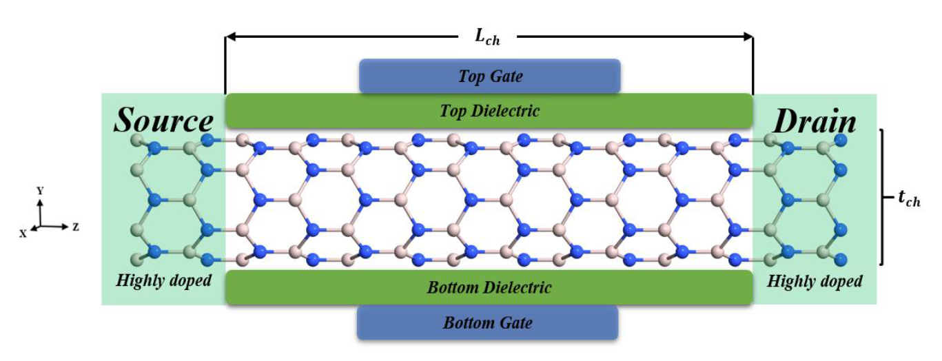
Figure 1: Schematic View of DG GaNNT MOSFETs
The construction of the GaNNT MOSFET model involves the utilization of intrinsic GaNNT material Lg£5 mn as the channel. The design setup depicted in Figure 1 employs double gates, to utilize strongly n- or p-doped GaNNT as electrodes. The optimal doping concentrations for the electrodes are determined to be 4×1013 cm-2 for n doping and 6×1013 cm-2 for p doping, respectively, as per the results of the test. Gate lengths were set to range from 1to 5 nm, in 1nm steps with SiO2, HfSiO4, HfO2, La2O3 and TiO2 as the oxide dielectric material. The range for the oxide thickness is established to be between 0.1 and 0.5 nm, with increments of 1 nm and the supply voltage (Vdd = Vb = 0.5 V) is adopted for each device.
The Ion and Ioff parameters are crucial metrics for evaluating the performance of logic transistors. A lower Ioff value signifies lower static power dissipation, while a higher Ion value indicates enhanced operational speed of the device. The values of Ion in n-type MOSFETs are achieved by measuring the Vg (on) = Vg (off) + Vdd conversely, The Ion values for p-type MOSFETs are typically determined at the Vg (on) = Vg (off) - Vdd. Here, the Vg (off) for all devices is zero. Figure 2a and b illustrates the transfer features of the n-type and p-type DG GaNNT FETs with the Lg sub-5 nm for different gate lengths, oxide dielectric material and oxide thickness by adjusting the gate voltage within the range of 0 to 1 V at supply voltage Vdd = Vb (off) - Vdd = Vb = 0.5 V. The Ids curves of n and p-type FETs at Lg = 5 nm with EOT = 0.1 nm show increased Ids with higher gate dielectric materials, as represented in Figure 2c and d.
In these figures, the Ids exhibits a greater magnitude when considering TiO2 as compared to other dielectric materials. An increase in the dielectric constant leads to an increase in the gate capacitance, thereby resulting in an increase in the inversion charge. An elevation in the inversion charge leads to a corresponding augmentation in the Ids due to the Low conduction band edge energy of FETs with a high dielectric material [22], implying that the process of conduction takes place at reduced energy levels, which makes the TiO2 and the La2O3 materials are better candidates as gate dielectric. At Lg = 5 nm and SiO2 dielectric layer, Figure 2e and f shows the decrease of driving current for the same gate voltage due to an increase in oxide thickness which leads to the reduction of gate capacitance [23].
Figure 2: Transfer Characteristics of DG GaNNT MOSFETs as a Function of (a, b) Gate Lengths, (c, d) Oxide Dielectric Material and (e, f) Oxide Thickness
The Ion/Ioff ratio serves as a key metric for evaluating the performance of a device, as it reflects the ability to achieve high performance (large Ion value) while minimising leakage power (small Ioff value). In this context, the value of Ion is determined when the Vg is equal to the threshold voltage (Vth), while the value of Ioff is determined when Vg is set to 0 V. According to Figure 3a, it can be observed that there is an increase in the Ion/Ioff ratio as the Lg is increased. The Ion/Ioff ratio exhibits an increase as the Lg is extended, because the Ion experiences an increase while the Ioff undergoes a drop. Moreover, it can be observed from Figure 3b that the Ion/Ioff ratio exhibits an upward trend as the dielectric constant increases. In a similar vein, it can be observed from Figure 3c that there is a notable decrease in the Ion/Ioff ratio as the tox is increased.

Figure 3: Ion/Ioff Ratio of DG GaNNT MOSFETs as a Function of (a) Gate Lengths, (b) Oxide Dielectric Material and (c) Oxide Thickness
In order to assess the effectiveness of gate control, the SS holds significant importance [24]. Enhanced gate control is correlated with a reduced SS in subthreshold region. Based on the formula SS = ¶Vg/¶ log Ids [25], the term SS represents the magnitude of the change in Vg required to induce a 1dec alteration in the current. According to the references [26,27] it is widely believed that long channel conventional MOSFETs, which typically have dimensions in the micrometer range, exhibit a fundamental SS limit of 60 mV/dec at ambient temperature. As depicted in Figure 4a, the SS values of the GaNNT MOSFETs exhibit a decreasing trend as the Lg increases. Notably, the SS value experiences a significant reduction from 95 to 78 mV/dec when Lg increases from 1 to 5 nm. The reduction of leakage from the source to the drain is achieved by raising the dielectric constant. This, in turn, effectively lowers the SS to 62 mV/dec when utilizing TiO2 as the dielectric material, as depicted in Figure 4b. The value of SS exhibits a progressive increase as the tox increases, eventually reaching a value of 98 mV/dec at a thickness of 0.5nm, as depicted in Figure 4c.
Figure 4: Subthreshold Swing of DG GaNNT MOSFETs as a Function of (a) Lg (b) Oxide Dielectric Material and (c) tox
Transconductance an additional significant element, plays a role in regulating the behavior of the gate inside the sub-threshold region. This can be expressed as the derivative of drain current with respect to gate voltage, denoted as (gm = ¶Ids/¶Vg) [24]. A greater value of gm is expected to enhance the capacity to control gates. Generally, the parameter gm exhibits an upward trend as both Lg and the dielectric constant increase, as depicted in Figure 5a and b. Conversely, gm experiences a decline when tox grows, as illustrated in Figure 5c.
Figure 5: Transconductance of DG SWAlNNT MOSFETs with Lg (a), Oxide Dielectric Material (b) and tox (c)
The characteristic of digital circuits is determined by their switching speed. The calculation of switching speed involves the utilization of the formula t = CtVdd/Ion [28]. In this equation, Ct represents the total capacitance, which is the combination of fringing capacitances (Cf) and channel capacitance (Cch) [24]. The determination of Cch can be accomplished by employing the formula Cch = ¶ Qch/W¶ Vg, where Qch denotes the total Mulliken charge of the central region and W represents the channel width. Based on the reference provided [24], it is assumed that the value of Cf, the channel capacitance, is twice that of Ci, the intrinsic channel capacitance. In general, it can be observed from Figure 6a and b that the parameter t demonstrates a decreasing pattern with increasing values of Lg and the dielectric constant. In contrast, the variable T exhibits an upward trend as the parameter tox increases, as depicted in Figure 6c.
Figure 6: Delay Time of DG GaNNT MOSFETs with Lg (a), Oxide Dielectric Material (b) and tox (c)
In the context of MOSFET applications, the PDP, denoted as PDP = Vdd Ion t, serves as a significant metric for evaluating the switching energy for digital circuits. In Figure 7, an analysis was conducted on the Power-Delay Product (PDP) of 2D-channel GaNNT MOSFETs for both n-type and p-type. The results indicate that the PDP exhibits a little drop as the Lg and dielectric constant increase, as shown in Figure 7a and b. Whereas, it increases with the tox, as depicted in Figure 7c.
Figure 7: PDP of DG GaNNT MOSFETs with Lg (a), Oxide Dielectric Material (b) and tox s (c)
The performance of GaNNT MOSFETs, both n-type and p-type MOSFETs, has been examined using the ab-initio DFT technique. This investigation focused on the influence of gate length, oxide dielectric material and oxide thickness. The simulation findings demonstrate that the Ion/Ioff ratio can be significantly enhanced by increasing the gate length and dielectric constant, as well as by decreasing the oxide thickness. For SS, the results indicate a notable enhancement in mitigating short channel effects as the gate length extended to 5 nm. In the context of t and PDP, it has been discovered that there is a notable enhancement in the short channel impact at the gate length increased, the dielectric constant is increased and the oxide thickness is decreased. This improvement is particularly prominent when considering a channel length of 5 nm for n-type devices. Therefore, GaNNT exhibits considerable promise as a channel material for the development of complementary MOSFETs suitable for both n-type and p-type devices.
Taylor, P.L. and O. Heinonen. A quantum approach to condensed matter physics. Cambridge University Press, 2002.
Taur, Y. and T.H. Ning. Fundamentals of modern VLSI devices. Cambridge University Press, 2021.
Yakobson, B.I. and P. Avouris. “Mechanical properties of carbon nanotubes.” Carbon nanotubes: synthesis, structure, properties and applications, Springer, 2001, pp. 287–327.
Snow, E., et al. “High-mobility carbon-nanotube thin-film transistors on a polymeric substrate.” Applied Physics Letters, vol. 86, no. 3, 2005, pp. 033105.
Franklin, N.R. et al. “Integration of suspended carbon nanotube arrays into electronic devices and electromechanical systems.” Applied Physics Letters, vol. 81, no. 5, 2002, pp. 913–915.
Palacios, J.J. “Electrons go ballistic.” Nature Physics, vol. 10, no. 3, 2014, pp. 182–183.
Javey, A. et al. “Ballistic carbon nanotube field-effect transistors.” Nature, vol. 424, no. 6949, 2003, pp. 654–657.
Franklin, A.D. et al. “Sub-10 nm carbon nanotube transistor.” Nano Letters, vol. 12, no. 2, 2012, pp. 758–762.
Pokropivny, V.V. “Non-carbon nanotubes (Review). Part 2. Types and structure.” Powder Metallurgy and Metal Ceramics, vol. 40, 2001, pp. 582–594.
Williams, D.P. et al. “Theory of GaN quantum dots for optical applications.” IEEE Journal of Selected Topics in Quantum Electronics, vol. 15, no. 4, 2009, pp. 1092–1103.
Marti, D. et al. “RF performance of AlGaN/GaN high-electron-mobility transistors grown on silicon (110).” Applied Physics Express, vol. 4, no. 6, 2011, p. 064105.
Goldberger, J. et al. “Single-crystal gallium nitride nanotubes.” Nature, vol. 422, no. 6932, 2003, pp. 599–602.
Zhi, C. et al. ” Materials Science and Engineering: R: Reports, vol. 70, no. 3–6, 2010, pp. 92–111.
Zhang, M. et al. “Theoretical interpretation of different nanotube morphologies among Group III (B, Al, Ga) nitrides.” Chemical Physics Letters, vol. 408, no. 1–3, 2005, pp. 145–149.
Soler, J.M. et al. “The SIESTA method for ab initio order-N materials simulation.” Journal of Physics: Condensed Matter, vol. 14, no. 11, 2002, p. 2745.
Brandbyge, M. et al. “Density-functional method for nonequilibrium electron transport.” Physical Review B, vol. 65, no. 16, 2002, p. 165401.
Datta, S. Electronic transport in mesoscopic systems. Cambridge University Press, 1997.
Perdew, J.P. et al. “Generalized gradient approximation made simple.” Physical Review Letters, vol. 77, no. 18, 1996, p. 3865.
Gao, S. and L. Yang. “Renormalization of the quasiparticle band gap in doped two-dimensional materials from many-body calculations.” Physical Review B, vol. 96, no. 15, 2017, p. 155410.
Zhong, H. et al. “Interfacial properties of monolayer and bilayer MoS₂ contacts with metals: beyond the energy band calculations.” Scientific Reports, vol. 6, no. 1, 2016, pp. 1–16.
Monkhorst, H.J. and J.D. Pack. “Special points for Brillouin-zone integrations.” Physical Review B, vol. 13, no. 12, 1976, p. 5188.
Mech, B.C. and J. Kumar. “Effect of high‐k dielectric on the performance of Si, InAs and CNT FET.” Micro & Nano Letters, vol. 12, no. 9, 2017, pp. 624–629.
Roy, K. et al. “Leakage current mechanisms and leakage reduction techniques in deep-submicrometer CMOS circuits.” Proceedings of the IEEE, vol. 91, no. 2, 2003, pp. 305–327.
Xu, L. et al. “Device performance and strain effect of sub-5 nm monolayer InP transistors.” Journal of Materials Chemistry C, vol. 10, no. 6, 2022, pp. 2223–2235.
Gowthaman, N. and V.M. Srivastava. “Mathematical modeling of electron density arrangement in CSDG MOSFET: a nano-material approach.” Journal of Materials Science, vol. 57, no. 18, 2022, pp. 8381–8392.
Abdul-Hussein, W.A. et al. “Designing sub-5 nm monolayer AlP MOSFETs.” Micro and Nanostructures, vol. 176, 2023.
Iqbal, M. et al. “Tailoring the electrical properties of MoTe₂ field effect transistor via chemical doping.” Superlattices and Microstructures, vol. 135, 2019, p. 106247.
Sun, X. et al. “Sub-5 nm monolayer arsenene and antimonene transistors.” ACS Applied Materials and Interfaces, vol. 10, no. 26, 2018, pp. 22363–22371.